During this year’s Hot Chips conference in Cupertino, California, AMD has presented what they’ve been able to achieve by using automated design tools (software) to rearrange the units inside its Bulldozer processors.
Before going ahead, you should read Part 1 and Part 2 of our AMD Hot Chips report.
Such a frequency would be catastrophically low for a CPU like AMD’s Bullzoder and despite the lower manufacturing costs and power consumption, not many would be interested in powering a personal computer with something like this.
The thing is that the Bulldozer die doesn’t have as many transistors as a Tahiti dies and as such will be able to reach much higher frequencies than the GPU dues to having a smaller and less complex die with a more modest power consumption.
Now we have a 2 GHz Bulldozer that has a small and economic die size and an improved power consumption level.
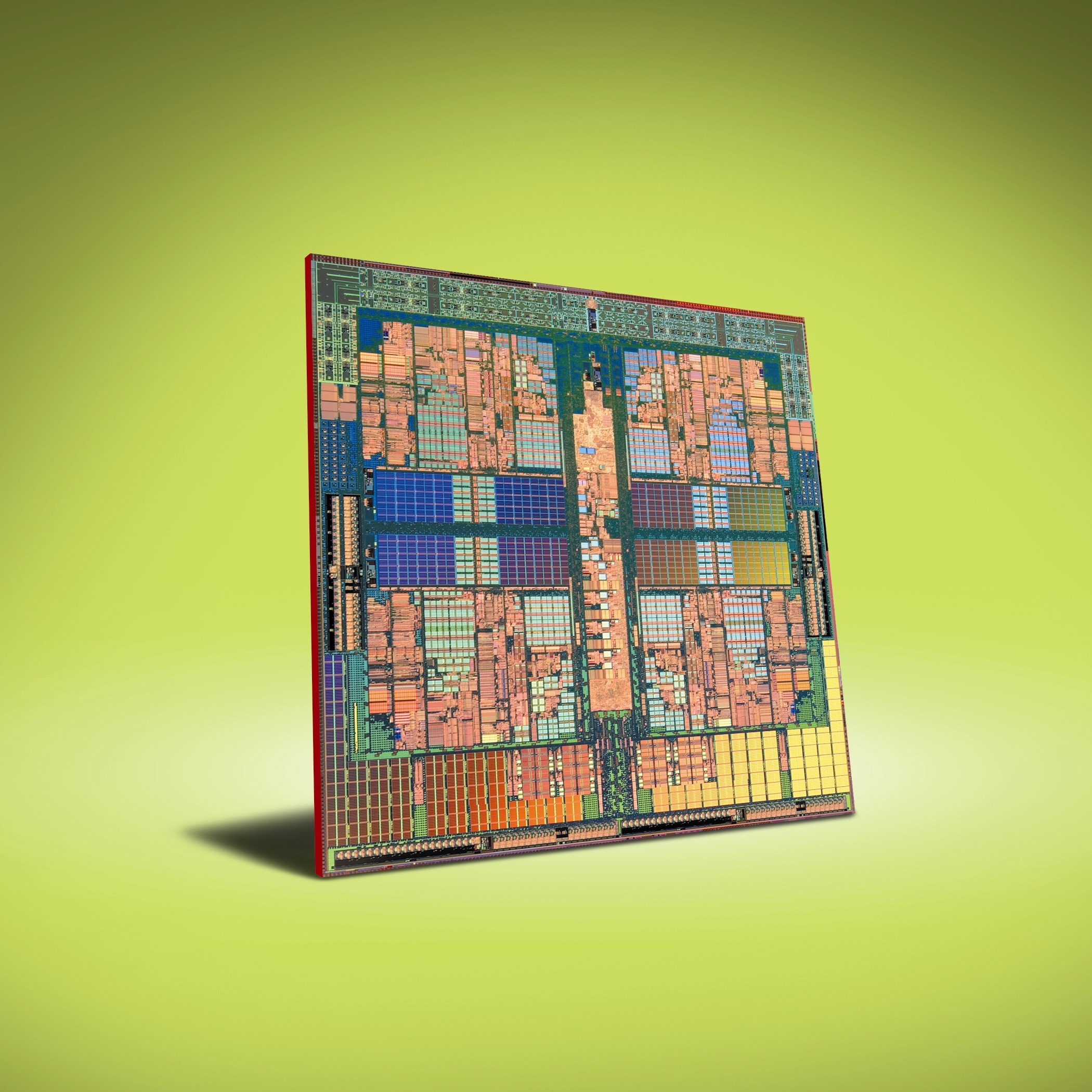
Interestingly enough, AMD is not aiming for a complete overhaul of its CPU die design.
Just like shown at the 2012 Hot Chips conference, the company is only redesigning parts of the CPU using the automated design tools. The units in question become much smaller and manifest lower power consumption.
AMD is showing a floating point unit (FPU) in the graphs made public at Hot Chips. The unit has been greatly reduced in size by using a different design solution (software using a High Density cell library).
A 30% reduction in die area is touted along with a 15% to 30% power consumption and these are results usually obtained by moving manufacturing from one node to another.
Getting a design from 32nm to 28nm manufacturing could take a whole year or even more.
Adding to the expected 20% ~ 30% die shrink and power consumption reduction that comes with such a move an additional 30% shrink and power improvement due to a tighter design would result in impressive results.
Such results would be comparable with a move to 20nm manufacturing.
The unknown is the frequency of such a design, but the company could opt for a differentiated clock design where some units work at a certain frequency and other units have a much higher functional frequency.
Extrapolating from AMD’s graphs, we could imagine a CPU that has more FPUs that are all kept fed by very fast dispatch units with efficient branch prediction.
It is all about balance and getting the right recipe, but what AMD is basically saying is that they are working with many solutions that offer good improvements and that combined will offer impressive results.
Via: AMD Experiments with Different CPU Design Methods Part 3
Tidak ada komentar:
Posting Komentar