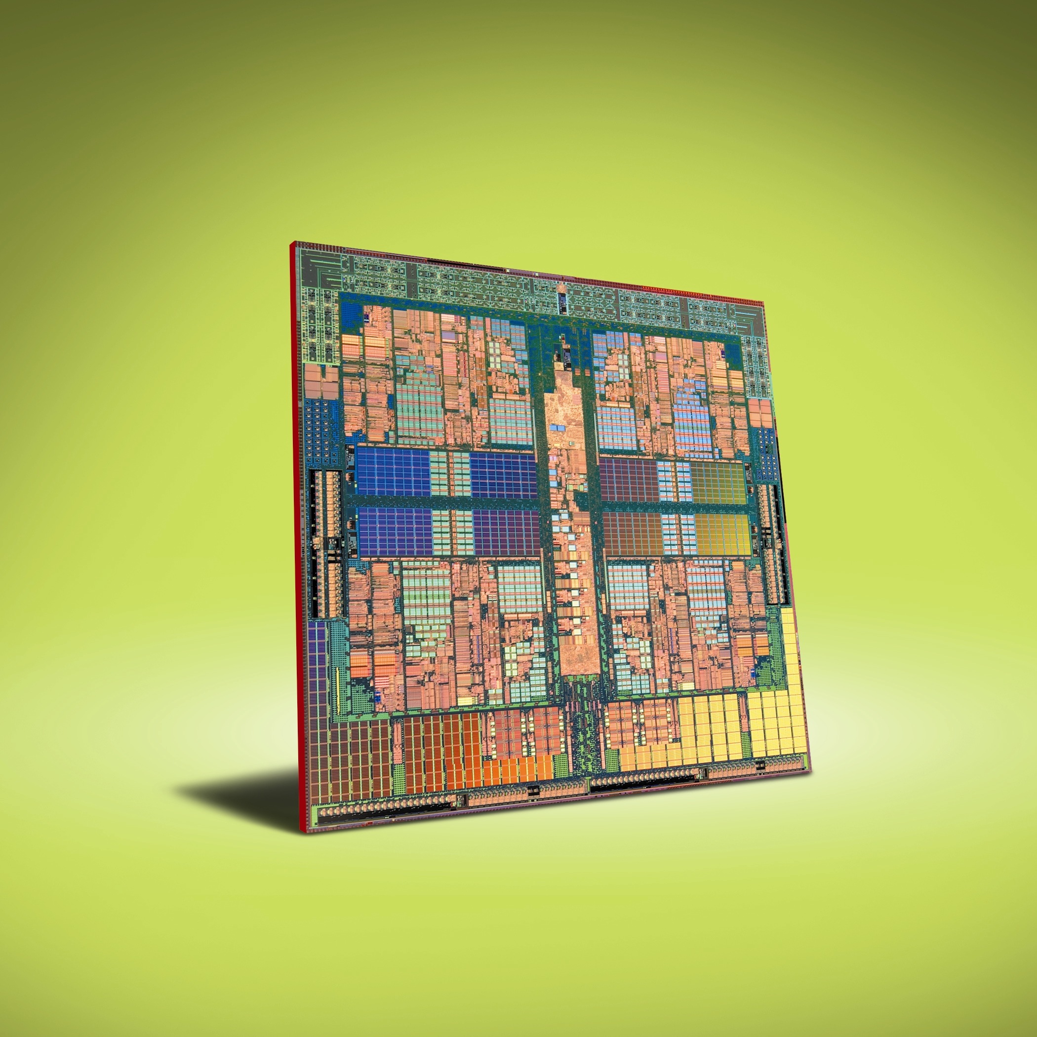
AMD has decided to concentrate on the bulk manufacturing process instead of the usual Silicon-on-Insulator (SOI) that has been the company’s main technology for the past eleven years.
When designing a high frequency microprocessor, the architect is not really concentrating on lowering the power consumption.
Some of the internal units that are literally getting very hot when heavily in use could pose a problem to the chip’s overall stability and ability to function.
Therefore the designers usually take the decision to move their position to a somewhat “cooler” are of the chip.
When designing a microchip with tens of millions of transistors or even billions, moving around some of the functional units might make the overall die size of the chip a whole lot bigger.
Back when Intel and AMD were fighting head to head for the absolute performance crown, some concessions about the die size and power consumption were made.
Basically the companies thought it was alright to have a 140 watts CPU TDP if that was what it took to win the benchmarks. The same goes for a 10% to 20% bigger die size.
This was back in the days when AMD has its own foundries and all the costs were managed by the company itself, but now that AMD is paying TSMC or GlobalFoundries for manufacturing their designs, the bigger die size would come with a significant increase in costs per chip.
Now the company is working with different foundries that are mostly using bulk manufacturing process and have various chip design tools at their disposal and it believes all this diversity comes with impressive potential.
Real all about these impressive AMD simulations and potential improvements in Part 2 of our AMD report that's coming later this week.
AMD Experiments with Different CPU Design Methods – Part 2.
Via: AMD Experiments with Different CPU Design Methods Part 1
Tidak ada komentar:
Posting Komentar